Altium Signal Integrity Tutorial
Maintaining stable voltages and suppressing noise ensures your PCB will operate as designed. P-CAD Signal Integrity can back annotate termination networks onto the board as a DRC marker.

Transmission Line And Pcb Track Design
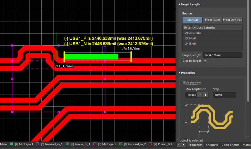
The timing requirements are met by matching the routed lengths of the signal paths.
Altium signal integrity tutorial. Altium Designer includes a signal integrity simulator that can be accessed during both the design capture and board layout phases of a design. Each component will be assigned a status as described in the following table. P-CAD Signal Integrity and Xtalk are designed for analyzing PCBs with consistent power andor ground planes.
And Zasio John J Right The First Time A Practical Handbook on High Speed PCB and System Design Volumes 1 and 2. When Signal Integrity issues are found Altium Designer shows you the effects of various termination options allowing you to find the best. P-CAD Signal Integrity can provide an INCASES EMC-WORKBENCH SULTAN file for extended EMC analysis.
This article will help you understand what causes signal integrity issues and if your board is likely to suffer from them. A unified PCB design software package that contains all the design and PDN analysis tools you need to build advanced electronics. I already gone through tutorial given by Altium.
Altium Designer includes plenty of other features beyond signal integrity analysis tools for high speed PCB design. Sir I am using Altium for PCB designing. To start lets review what COM is and a high level overview of how COM is calculated.
Signal Integrity screening is built into the Altium Designer design rules system allowing you to check for Signal Integrity violations as part of the normal board DRC Design Rule Checking process. 13 1 WP-SGNLNTGRY-13 Introduction Digital designs have not traditionally suffered by issues associated with transmission line effects. If youve enjoyed this power integrity tutorial and you want to see how the best layout tools can help you tackle signal and power integrity problems talk to an Altium expert today.
It covers setting up design parameters like design rules and Signal Integrity models starting up Signal Integrity from the Schematic and PCB Editors configuring the tests to be used in the net screening analysis running further analysis on selected nets terminating the signal line setting preferences and working with the. If possible give me small video tutorial or give me some helpful links. The PCB editor in Altium Designer has these capabilities.
Interference Amplitude Distortion Ive talked about COM and channel analysis in previous blogs and Id like to continue the discussion with more visual aids and some example code to enable readers to do some analysis themselves. The Signal Integrity panel is the control center for performing signal integrity analysis on a design. Pre-layout Signal Integrity Analysis.
From that I get only idea about IBIS Model. Or alternatively What is the optimum slew and drive settings to use for FPGA pins driving signals D310 This tutorial relates to the example project Nbp-28PrjPcb which can be found in the ExamplesSignal IntegrityNbp-28 folder of the Altium Designer examples. Now I want to learn SIsignal integrity issue.
The layout tools are built on the same rules-driven design engine and data model as the signal integrity features allowing these tools to work within your design constraints. Whether you are working with MIPI physical layer specifications or other signaling standards the routing and layout tools in Altium Designer are ideal for creating. Whats needed is the ability to detect and rectify potential signal integrity problems particularly impedance mismatches early in the design cycle.
The signal integrity can be managed through controlled impedance routing which is achieved through careful design of both the PCB stackup and the routing widths to be used on each layer. TU0113 Performing Signal Integrity Analyses Version v13 Mar 11 2008 3 components including those with models already defined and the model information will be displayed in the Model Assignments dialog. Because C-PHY works with edge transitions at the receiver rather than typical signal levels it is less sensitive to losses in the signal level than typical signaling techniques.
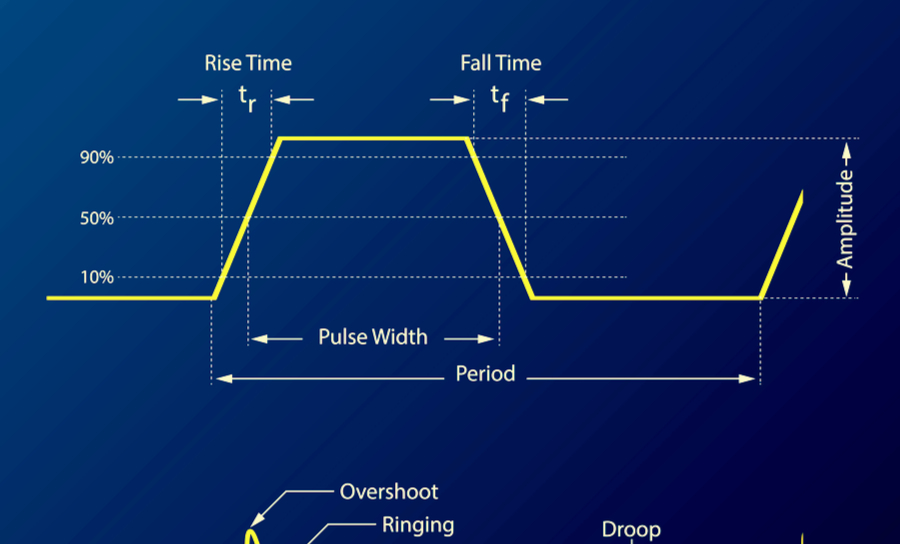
COM is a signal-to-noise ratio of voltage at a point in time. It will also discuss the two design approaches you must employ to minimizing potential SI issues - matching component impedances and controlled impedance routing. But not getting whole idea so give me small tutorials related to SIsignal integrity.
At lower frequencies the signals remain within data characterization and the. Power integrity and signal integrity are some of the most important aspects in many PCBs. Basic Principles of Signal Integrity December 2007 ver.
It enables you to screen all nets in a design against various defined signal integrity rules in order to quickly identify problematic nets. The Signal Integrity panel is used to configure and control the signal integrity analysis process. This example is based on the daughterboard NBP28.
This tutorial looks at performing Signal Integrity SI analyses.

16 Altium Designer Spice Simulation I Signal Integrity Youtube
High Speed Pcb Design Analysis Simulations And Signal Integrity Checks Pcb Design Blog Altium
The Best High Speed Design Tools In Altium Designer

Signal Integrity Online Documentation For Altium Products