Cadence Noise Simulation Tutorial
0 vsource dc3 o Gnd gnd. 0 vsource dc0 o v1 A 0 vsource dcvs o dcs dc paramvs start0 stop3 step001 This assumes your input node is called A.
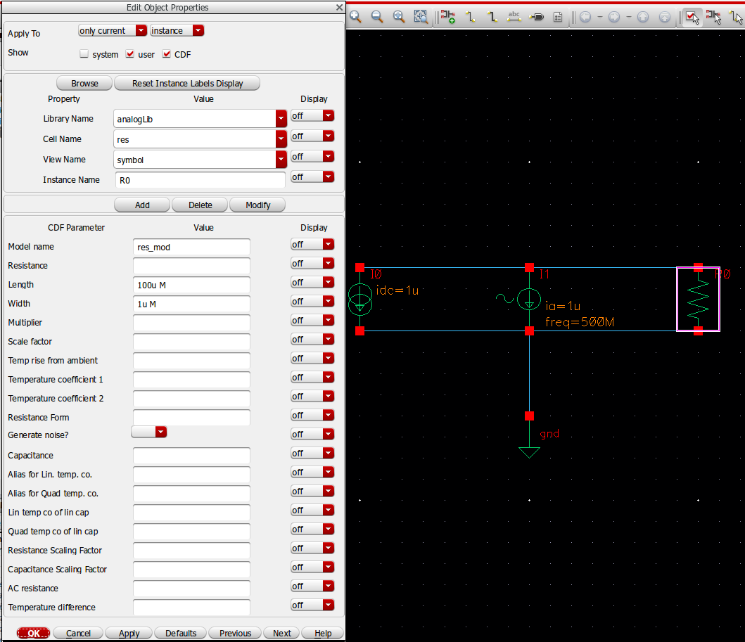
Resistor Noise Simulation By Transient Analysis Custom Ic Design Cadence Technology Forums Cadence Community
This Tutorial LAB describes how to use SpectreRF in Analog Design Environment to simulate the parameters which are important in design verification of a mixer.
Cadence noise simulation tutorial. It will start simulation. First change the TB created in 321 by placing a vdc at the input of. Cadence SPECTRE Noise Figure simulation.
KVCO simulation PSS Periodic Steady State Analysis Any Verilog-A models are not allowed in the simulation bench PSS does not support Verilog-A. Look for the chapter of Simulating Low noise amplifier and look at the section of Linear Two-Port Noise Analysis with S-Parameters. When Cadence netlists the schematic to produce something to simulate it will assign net names.
Configure the Local Oscillator LO and output ports as before. This is a very basic tutorial for beginners. Simulating DC and Timing Characteristics 7 o simulator langspectre o global gnd.
As an example in this tutorial DC simulation will be used to plot the inverters characteristic curve. Two tutorials Tutorial 1 and Tutorial 2 have been placed on the course website that walk through the configuration and basic use of Cadence and the IBM process. Cadence Tutorial 1 Schematic Entry and Circuit Simulation 5 Sweep range type 0 for start and 15 for stop.
It explains transient analysis in cadence with examples. Cadence Virtuoso Tutorial version 61 University of Southern California Last Update. A We will use Cadence for schematic capture simulation and layout of all circuits in this class.
Wire up the circuit dont forget to wire up the substrate terminal of the MOSFET. Simulate the noise spectral density R â è ç 6Hz and the. It is being or has been removed from the documentation in MMSIM121.
Simulation results Calculate the noise at each input voltage and average the results Allows users to asses the accuracy of the simulation results The total inferred noise is 442mV rms for noisefmax of 500GHz Calculating Dynamic Comparator Noise with Transient Noise Alternative transient noise. In 18-723 we will use Cadence tools to do transistor-level circuit design and simulation. Cadence contains an entire design framework for IC design including schematic capture layout circuit simulation.
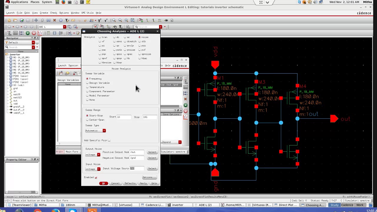
Enable the PSS analysis see image below The only tones listed in the Fundamental Tones section should be the local oscillators. O parameters vs0 o vdd vdd. To characterize a mixer the following figure of merits are usually simulated and measured.
For Sweep Type click and select Linear then select Step Size and enter 0005 ie. RF to IF Conversion Gain 3. Noise and NF 4.
Click on the Netlist and Run Simulation button looks like a green light on the right or go to Simulation - Netlist and Run. Cadence SPECTRE IP3 simulation. Configure the input port psin source see image below.
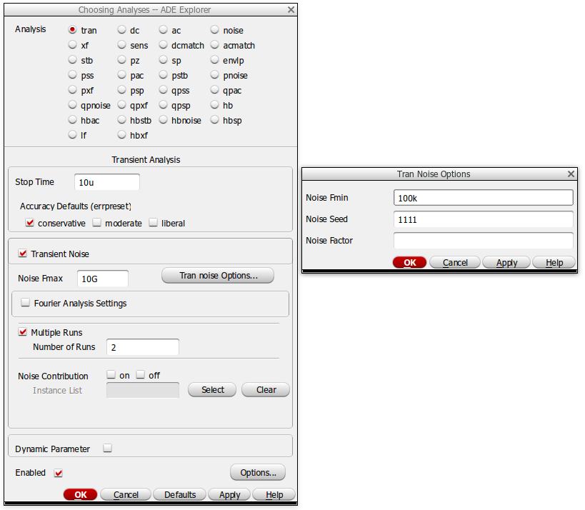
Do tran analysis first to estimate the VCO frequency at the fixed Vctrl as the Beat frequency. Note an output capacitance is not needed since. Transient Noise Simulation Create a new transient simulation open the transient options form then add the transient noise parameters to the Additional Options field.
Resistance 50 ohm set as desired type dc. Oct 2015 EE209 Fall 2015. To run the simulation click the.
The PLL Noise Aware flow is no longer recommended. Schmitt Trigger Hysteresis Provides Noise-free Switching and Output Schmitt trigger hysteresis is easy to incorporate with standard op-amp models in your circuit design tools. The first one combines a PSS analysis where one tone is treated as a large-signal and a PAC analysis where the other tone is treated as small-signal the second one uses a QPSS analysis treating both input tones as large signalsThere is actually a third way to calculate the IP3 using the Rapid IP3 function but it will.
Cadence Tutorial 16 Fig. 16 ADE after setup Now we can finally simulate. Press w to use the wire tool and its pretty easy.
A common-source amplifier is used as. You should check your Virtuoso. You will need to wait for a while.
You may also want to look at transienttransient noise. Make sure the VCO works by setting the Initial Condition. Tutorial on Cadence Design Tools.
Cadence and SpectreRF Tutorial By Albert Jerng 021305 Introduction This tutorial will introduce the use of Cadence and SpectreRF for performing circuit simulation in 6776. There are two ways to simulate IP3. The characteristic curve can be helpful in determining the inverters threshold voltage noise margins and its gain.
Cadence 018μm CMOS PDK gpdk180 Cadence Version 615 Yongsuk Choi Marvin Onabajo This tutorial provides a quick introduction to the use of Cadence tools for schematic simulation layout creation layout verification and post-layout simulation of amplifiers. Amplifier Simulation Tutorial Design Kit. Cadence will try to snap to points that are attachable or you can double-click to terminate a wire mid-route.
5mV in the field of Step Size.
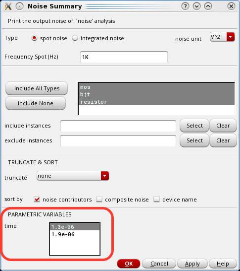
Print Noise Summary After Analysis During Tran Custom Ic Design Cadence Technology Forums Cadence Community
Cadence Ic615 Virtuoso Tutorial 9 Noise Analysis In Cadence Adel Youtube
Resistor Noise Simulation By Transient Analysis Custom Ic Design Cadence Technology Forums Cadence Community
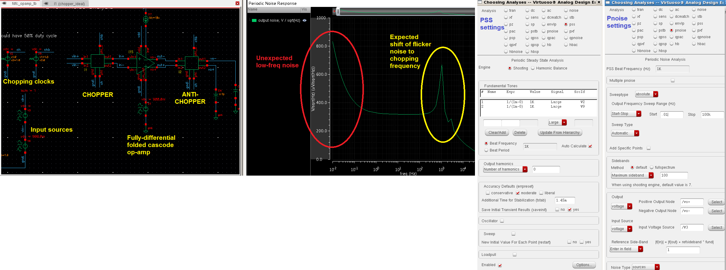
Noise Simulation Of Chopper Amplifier Using Pss Pnoise Custom Ic Design Cadence Technology Forums Cadence Community